| CPC G06F 3/0412 (2013.01) [G06F 3/0443 (2019.05); G06F 3/0446 (2019.05); G06F 3/04164 (2019.05); H10K 10/476 (2023.02); H10K 10/88 (2023.02); H10K 50/844 (2023.02); H10K 59/40 (2023.02); H10K 71/621 (2023.02); G02F 1/136286 (2013.01); G06F 2203/04102 (2013.01); G06F 2203/04103 (2013.01); G06F 2203/04111 (2013.01); H10K 59/1213 (2023.02); H10K 2102/311 (2023.02)] | 18 Claims |
|
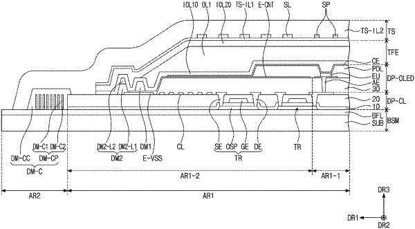
1. A display device comprising:
a base member;
a circuit layer disposed on the base member;
a display layer disposed on the circuit layer and comprising an organic light emitting diode;
a thin film encapsulation layer disposed on the display layer and comprising a first inorganic thin film, an organic thin film, and a second inorganic thin film sequentially stacked; and
a touch sensor layer disposed directly on the thin film encapsulation layer,
wherein:
the touch sensor layer comprises a first conductive layer disposed on the thin film encapsulation layer, a first insulating layer disposed on the first conductive layer, a second conductive layer disposed on the first insulating layer, and a second insulating layer disposed on the second conductive layer;
a first region overlapping the circuit layer and a second region non-overlapping the circuit layer are defined in the base member;
the second insulating layer overlaps the first region and extends to cover at least a portion of the second region of the base member; and
the second insulating layer directly contacts a portion of the thin film encapsulation layer and a portion of the circuit layer.
|