| CPC G06F 13/1684 (2013.01) [G06F 1/06 (2013.01); G06F 13/1647 (2013.01)] | 20 Claims |
|
1. An apparatus, comprising:
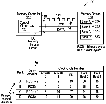
a memory interface circuit configured to couple to a memory device via an interface having a command bus that is clocked by a command clock signal, wherein the memory device includes a plurality of banks; and
a control circuit coupled to the memory interface circuit and configured to initiate a multi-bank memory operation by scheduling a sequence of bank-specific commands to be sent over the command bus to the memory device, wherein the bank-specific commands for a given memory bank include:
a first activate command, followed by a second activate command two cycles of the command clock signal later; and
a read/write command that follows the second activate command by at least a minimum timing parameter specified for the memory device, wherein the read/write command specifies a type of operation to be performed; and
wherein every other read/write command during the multi-bank memory operation is scheduled to be delayed beyond the minimum timing parameter, and
wherein remaining read/write commands are scheduled to not be delayed beyond the minimum timing parameter.
|