| CPC G06F 1/06 (2013.01) [H03K 3/017 (2013.01); H03K 19/20 (2013.01)] | 12 Claims |
|
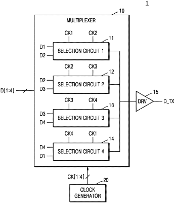
1. A transmitter circuit that receives parallel signals and outputs a serial signal in response to the parallel signals, the transmitter circuit comprising:
a clock generator configured to generate first clock signals having different respective phases;
a multiplexer including a plurality of selection circuits respectively configured to selectively provide at least two of the parallel signals to an output node in response to at least two of the first clock signals; and
an output driver configured to generate the serial signal by amplifying a signal the output node,
wherein each selection circuit of the plurality of selection circuits comprises:
a first P-type transistor configured to precharge the output node in response to detecting a first parallel signal among the parallel signals having a first logic level and a second parallel signal among the parallel signals having the first logic level; and
a first N-type transistor configured to discharge the output node in response to detecting the first parallel signal having a second logic level and a second parallel signal having the second logic level.
|