| CPC G05F 3/265 (2013.01) [G05F 3/222 (2013.01); G05F 3/225 (2013.01); G05F 3/30 (2013.01); H03F 3/45179 (2013.01)] | 4 Claims |
|
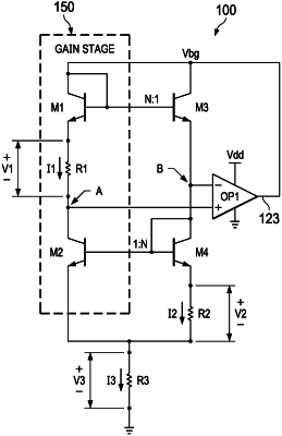
1. A bandgap reference circuit, comprising:
a first bipolar junction transistor (BJT) having a first emitter, a first base, and a first collector, the first base shorted to the first collector;
a second BJT coupled to the first BJT via a first resistor, the second BJT having a second emitter, a second base, and a second collector;
a third BJT coupled to the first BJT, the third BJT having a third emitter, a third base, and a third collector, the third base coupled to the first base;
a fourth BJT coupled to the third BJT, the fourth BJT having a fourth emitter, a fourth base, and a fourth collector, the fourth base shorted to the fourth collector, and the fourth base coupled to the second base;
a second resistor coupled to the fourth emitter;
a third resistor coupled to the second resistor and to the second emitter; and
an operational amplifier having a first input coupled to the first resistor and the second collector, a second input coupled to the third emitter and the fourth collector, and an output coupled to the first and third collectors.
|