US 11,914,306 B2
Predicting defect rate based on lithographic model parameters
Erik A. Verduijn, Leuven (BE); Ulrich Karl Klostermann, Munich (DE); Ulrich Welling, Aschheim/Dornach (DE); Jiuzhou Tang, Aschheim/Dornach (DE); and Hans-Jürgen Stock, Dachau (DE)
Assigned to Synopsys, Inc., Sunnyvale, CA (US)
Filed by Synopsys, Inc., Mountain View, CA (US)
Filed on Oct. 16, 2020, as Appl. No. 17/072,568.
Claims priority of application No. 19204192 (EP), filed on Oct. 18, 2019.
Prior Publication US 2021/0116817 A1, Apr. 22, 2021
Int. Cl. G03F 7/00 (2006.01); G06F 30/23 (2020.01); G03F 7/004 (2006.01); G06F 17/15 (2006.01)
CPC G03F 7/7065 (2013.01) [G03F 7/0045 (2013.01); G06F 17/15 (2013.01); G06F 30/23 (2020.01)] 20 Claims
OG exemplary drawing
 
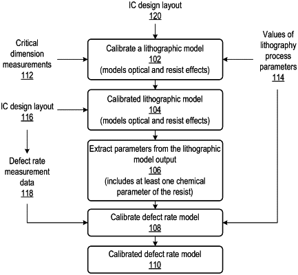
1. A method, comprising:
using a calibrated lithographic model to generate a lithographic model output based on simulating a lithography process for an integrated circuit (IC) design layout;
extracting, by a processor, at least a chemical parameter from the lithographic model output, wherein the chemical parameter is an inhibitor concentration; and
using a calibrated defect rate model to predict a defect rate for the IC design layout based on the chemical parameter.