| CPC G02F 1/133603 (2013.01) [G02F 1/133526 (2013.01); G02F 1/133621 (2013.01); G02F 2203/02 (2013.01)] | 4 Claims |
|
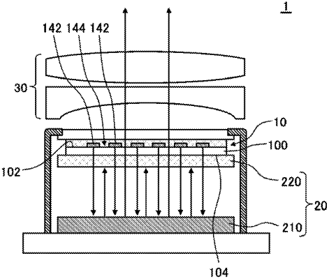
1. A display device comprising:
a light-emitting device comprising a plurality of light-emitting units and a light-transmitting unit located between the light-emitting units adjacent to each other;
a reflective liquid crystal element; and
an optical member,
wherein the light-emitting device is located between the reflective liquid crystal element and the optical member,
wherein the plurality of light-emitting units emit light toward the reflective liquid crystal element,
wherein the light emitted from the plurality of light-emitting units is reflected by the reflective liquid crystal element, transmitted through the light-transmitting unit of the light-emitting device, and formed into an image by the optical member,
wherein the reflective liquid crystal element is located within a depth of field of the optical member, and
wherein the plurality of light-emitting units of the light-emitting device are located outside the depth of field of the optical member.
|