| CPC G02F 1/133512 (2013.01) [G02F 1/13338 (2013.01); G02F 1/13439 (2013.01); G02F 1/134309 (2013.01)] | 20 Claims |

|
1. An optical path control member comprising:
a first substrate;
a first electrode disposed on the first substrate;
a second substrate disposed on the first substrate;
a second electrode disposed under the second substrate;
a photoconversion unit disposed between the first electrode and the second electrode; and
an adhesive layer disposed between the first electrode and the photoconversion unit,
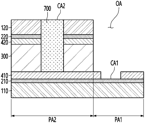
wherein the second substrate includes at least one hole penetrating the second substrate and the second electrode,
wherein an electrode connection part connected to a side surface of the second electrode is disposed inside the hole,
wherein the second substrate includes an open region,
wherein the hole is disposed on a protruding portion of the second substrate protruding by the open region, and
wherein the adhesive layer is removed from one region on the first substrate corresponding to the open region to expose the first electrode.
|