US 11,914,184 B2
Optically functional multilayer structure suitable for large area illumination and related method of manufacture
Antti Keränen, Oulunsalo (FI); Tero Heikkinen, Oulunsalo (FI); Pasi Korhonen, Oulunsalo (FI); Pälvi Apilo, Oulunsalo (FI); Mikko Heikkinen, Oulunsalo (FI); Jarmo Sääski, Oulunsalo (FI); Paavo Niskala, Oulunsalo (FI); Ville Wallenius, Oulunsalo (FI); Heikki Tuovinen, Oulunsalo (FI); Janne Asikkala, Oulunsalo (FI); Taneli Salmi, Oulunsalo (FI); Suvi Kela, Oulunsalo (FI); Outi Rusanen, Oulunsalo (FI); Johanna Juvani, Oulunsalo (FI); Mikko Sippari, Oulunsalo (FI); Tomi Simula, Oulunsalo (FI); Tapio Rautio, Oulunsalo (FI); Samuli Yrjänä, Oulunsalo (FI); Tero Rajaniemi, Oulunsalo (FI); Simo Koivikko, Oulunsalo (FI); Juha-Matti Hintikka, Oulunsalo (FI); Hasse Sinivaara, Oulunsalo (FI); Vinski Bräysy, Oulunsalo (FI); Olimpia Migliore, Oulunsalo (FI); and Juha Sepponen, Oulunsalo (FI)
Assigned to TACTOTEK OY, Oulunsalo (FI)
Filed by TactoTek Oy, Oulunsalo (FI)
Filed on Jun. 22, 2023, as Appl. No. 18/339,467.
Application 18/339,467 is a continuation in part of application No. 18/326,110, filed on May 31, 2023.
Application 18/326,110 is a continuation of application No. 17/945,247, filed on Sep. 15, 2022, granted, now 11,703,627.
Application 17/945,247 is a continuation of application No. 17/856,959, filed on Jul. 2, 2022, granted, now 11,500,142, issued on Nov. 15, 2022.
Prior Publication US 2024/0004120 A1, Jan. 4, 2024
This patent is subject to a terminal disclaimer.
Int. Cl. F21V 8/00 (2006.01); G02B 5/08 (2006.01)
CPC G02B 6/0031 (2013.01) [G02B 6/004 (2013.01); G02B 6/0021 (2013.01); G02B 6/0036 (2013.01); G02B 6/0041 (2013.01); G02B 6/0043 (2013.01); G02B 6/0051 (2013.01); G02B 6/0055 (2013.01); G02B 6/0061 (2013.01); G02B 6/0065 (2013.01); G02B 6/0068 (2013.01); G02B 6/0073 (2013.01); G02B 6/0083 (2013.01); G02B 5/0883 (2013.01)] 30 Claims
OG exemplary drawing
 
1. An integrated optically functional multilayer structure suitable for large area dynamic illumination, comprising:
a flexible, substrate film arranged with a circuit design comprising at least a number of electrical conductors; and
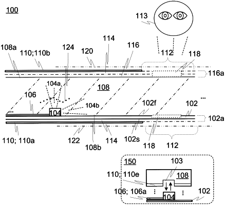
a plurality of top-emitting, bottom-installed light sources provided upon a first side of the substrate film to internally illuminate at least a portion of the structure for external perception via associated outcoupling areas,
wherein for each light source of the plurality of light sources there is,
an optically transmissive plastic layer, provided upon the first side of the substrate film, said plastic layer at least laterally surrounding or neighbouring, the light source,
a reflector design comprising at least one material layer, provided at least upon the light source and configured to reflect, the light emitted by the light source and incident upon the reflective layer towards the plastic layer; and
at least one further, material layer, in contact with the reflector design, said at least one further material layer having a lower refractive index than the plastic layer.