| CPC G02B 1/04 (2013.01) [G02B 5/0215 (2013.01); H10K 50/84 (2023.02); H10K 50/858 (2023.02); G06F 1/1609 (2013.01); H10K 59/122 (2023.02); H10K 2102/00 (2023.02)] | 15 Claims |
|
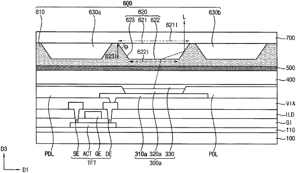
1. A display device comprising:
a first substrate;
a first electrode disposed on the first substrate;
an emission layer disposed on the first electrode;
a second electrode disposed on the emission layer;
a high refractive index member disposed on the second electrode, the high refractive index member overlapping the emission layer, and having a first refractive index;
a low refractive index member disposed between the high refractive index member and the emission layer and having a second refractive index smaller than the first refractive index;
a capping member disposed between the low refractive index member and the emission layer; and
a second substrate overlapping at least a portion of the first substrate and disposed on the high refractive index member,
wherein the high refractive index member has a closed shape, and
the low refractive index member and the second substrate entirely cover the closed shape of the high refractive index member.
|