| CPC G01T 1/244 (2013.01) [G01T 1/026 (2013.01); G01T 1/1606 (2013.01); G01T 1/242 (2013.01); G01T 1/245 (2013.01); G01T 1/247 (2013.01); G01T 7/00 (2013.01); H10B 80/00 (2023.02)] | 20 Claims |
|
1. A radiation detection device comprising:
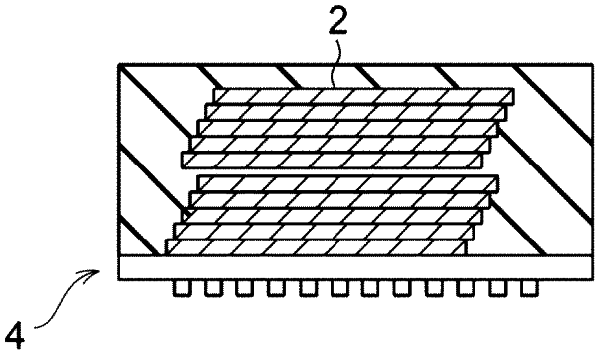
a first memory module mounted on a first substrate electrically connected to a first connection interface, the first memory module including a plurality of first memory chips that are vertically stacked on top of one another and mounted on the first substrate, each of the first memory chips including a plurality of vertically-stacked and non-volatile first memory cells;
a second memory module mounted on a second substrate that is above the first memory module and electrically connected to a second connection interface, the second memory module including a plurality of second memory chips that are vertically stacked on top of one another and mounted on the second substrate, each of the second memory chips including a plurality of vertically-stacked and non-volatile second memory cells; and
a controller electrically connected to the first and second connection interfaces and configured to detect gamma rays according to a data inversion or a threshold voltage change of at least some of the non-volatile memory cells in the first and second memory modules.
|