| CPC G01R 33/02 (2013.01) [G01R 33/0023 (2013.01)] | 14 Claims |
|
1. A magnetic field sensor package, comprising:
a sensor housing;
a first sensor chip having an integrated first differential magnetic field sensor circuit, the first sensor chip being arranged in the sensor housing, wherein the integrated first differential magnetic field sensor circuit is configured to generate a first output signal comprising first signal pulses with a pulse width modulation (PWM) coding based on a varying magnetic field;
a second sensor chip having an integrated second differential magnetic field sensor circuit, the second sensor chip being arranged in the sensor housing, wherein the integrated second differential magnetic field sensor circuit is configured to generate a second output signal comprising second signal pulses with the PWM coding based on the varying magnetic field;
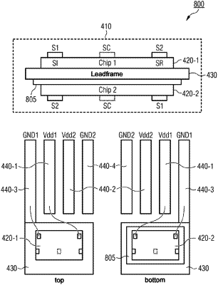
a common leadframe arranged in the sensor housing and interposed between the first sensor chip and the second sensor chip, wherein the common leadframe includes a common output signal terminal configured to output the first output signal and the second output signal from the common leadframe, wherein the first output signal and the second output signal are combined to form a common output signal; and
an insulating layer arranged in the sensor housing interposed between the first sensor chip and the common leadframe, wherein the first sensor chip is coupled to the common leadframe via the insulating layer,
wherein the first sensor chip and the second sensor chip are coupled to the common leadframe within the sensor housing, wherein the second sensor chip is directly in contact with the common leadframe,
wherein the first sensor chip is arranged on a first side of the common leadframe and the second sensor chip is arranged on a second side of the common leadframe, the second side being oppositely arranged with respect to the first side,
wherein the insulating layer electrically insulates the first sensor chip from the common leadframe such that the first sensor chip and the second sensor chip are galvanically decoupled from each other, and
wherein the first sensor chip and the second sensor chip are redundant sensor chips.
|