| CPC C23C 16/52 (2013.01) [C23C 16/4584 (2013.01); H01L 21/67303 (2013.01)] | 11 Claims |
|
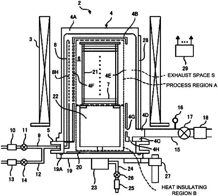
1. A substrate processing apparatus comprising:
a boat on which substrates are placed;
a process furnace comprising a reaction tube into which the boat is to be inserted and a rotator configured to rotate the boat by placing the boat on a rotating shaft when the boat is inserted in the reaction tube, wherein a film is formed on the substrates placed on the boat in the reaction tube;
a substrate transport device configured to transfer the substrates into the boat; and
a controller configured to control the substrate transport device, wherein the controller is further configured to store information on a difference between a rotation axis of the rotating shaft and a virtual center axis of the reaction tube measured in advance so that the substrates are transferred into the boat by the substrate transport device referring to the virtual center axis.
|