| CPC C23C 16/45578 (2013.01) [C23C 16/45546 (2013.01); C23C 16/45595 (2013.01); H01L 21/67 (2013.01); H01L 21/673 (2013.01)] | 8 Claims |
|
1. A semiconductor manufacturing apparatus comprising:
a process chamber;
a boat disposed in the process chamber and including a support member that is configured to support a plurality of substrates arranged in a first direction;
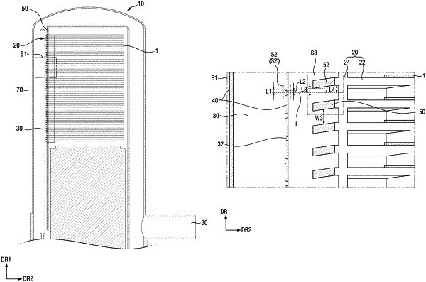
an inner tube enclosing the boat and including a slit formed along a side wall of the boat; and
a nozzle tube disposed in the process chamber, the nozzle tube including a side wall having a plurality of opening parts, the side wall of the nozzle tube including a nozzle extending in the first direction,
wherein the nozzle includes a gas injection port defined by one opening part along the side wall of the nozzle tube,
the gas injection port includes an inlet through which process gas flows in from the nozzle and an outlet through which the process gas is directed towards the slit,
a width of the inlet in the first direction is different from a width of the outlet in the first direction, and
the slit is inclined in an acute angle with respect to a second direction perpendicular to the first direction.
|