| CPC H10B 43/27 (2023.02) [H01L 29/78642 (2013.01); H10B 43/10 (2023.02); H10B 43/35 (2023.02)] | 21 Claims |
|
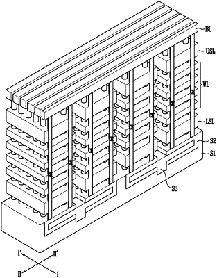
[ 21. A semiconductor device comprising:
a stack comprising conductive layers and insulating layers that are alternately stacked; and
a slit insulating layer passing through the stack in a stacking direction, an upper flat surface of the slit insulating layer comprising a first main pattern having a first edge and a second edge extending in a first direction, a first protruding pattern protruding from the first edge at a one end of the first main pattern in a second direction crossing the first direction, a second protruding pattern protruding from the second edge at the one end of the first main pattern in the second direction, a third protruding pattern protruding from the first edge at the other end of the first main pattern in the second direction, and a fourth protruding pattern protruding from the second edge at the other end of the first main pattern in the second direction,
wherein a lower flat surface of the slit insulating layer has a shape in which a center portion thereof and an end portion thereof have substantially the same width, and
wherein at least one of the first to fourth protruding patterns of the upper flat surface decreases in size towards the lower flat surface. ]
|