| CPC H10N 50/80 (2023.02) [H10B 61/00 (2023.02); H10N 50/01 (2023.02)] | 14 Claims |
|
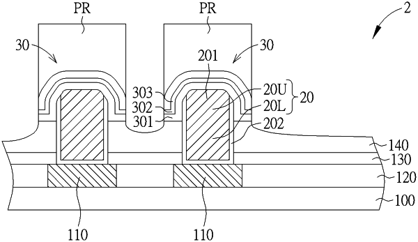
1. A semiconductor memory device, comprising:
a substrate comprising a conductor region thereon;
an interlayer dielectric layer on the substrate;
a conductive via electrically connected to the conductor region, wherein the conductive via comprises a lower portion embedded in the interlayer dielectric layer and an upper portion protruding from a top surface of the interlayer dielectric layer, wherein the upper portion has a rounded top surface, wherein the upper portion has a width that is equal to or smaller than a width of the lower portion; and
a storage structure conformally covering the rounded top surface.
|