US 11,895,922 B2
Etching method for forming vertical structure, electronic device including vertical structure formed by the etching method, and method of manufacturing the electronic device
Choongho Rhee, Anyang-si (KR); Sungchan Kang, Hwaseong-si (KR); and Yongseop Yoon, Seoul (KR)
Assigned to SAMSUNG ELECTRONICS CO., LTD., Suwon-si (KR)
Filed by SAMSUNG ELECTRONICS CO., LTD., Suwon-si (KR)
Filed on Apr. 7, 2021, as Appl. No. 17/224,254.
Claims priority of application No. 10-2020-0153081 (KR), filed on Nov. 16, 2020.
Prior Publication US 2022/0158074 A1, May 19, 2022
Int. Cl. H10N 30/30 (2023.01); G01L 1/16 (2006.01); H10N 30/082 (2023.01)
CPC H10N 30/302 (2023.02) [G01L 1/16 (2013.01); H10N 30/082 (2023.02); H10N 30/306 (2023.02)] 21 Claims
OG exemplary drawing
 
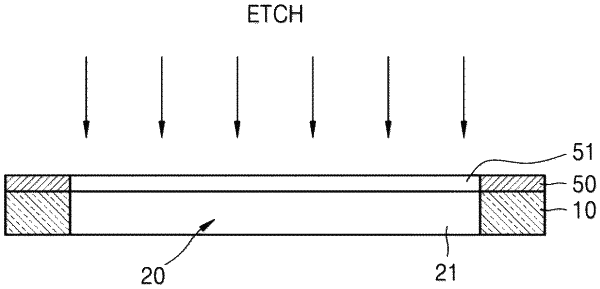
1. An etching method for forming a vertical structure, the etching method comprising:
positioning a mask on a substrate, an opening pattern of the mask comprising a compensation pattern that is disposed at a corner of the opening pattern and is indented from the corner of the opening pattern towards an outer boundary of the mask; and
forming the vertical structure on the substrate through the opening pattern of the mask by a dry etching process.