| CPC H10K 71/15 (2023.02) [C09K 11/616 (2013.01); H10K 50/15 (2023.02); H10K 50/16 (2023.02); H10K 50/17 (2023.02); H10K 71/00 (2023.02)] | 18 Claims |
|
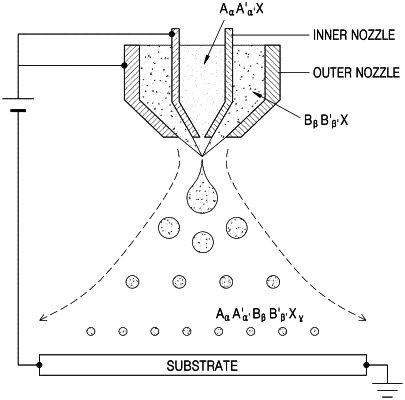
1. A method of forming a perovskite thin film, the method comprising:
preparing a substrate;
spraying a first solution of a first perovskite compound precursor through an inner nozzle of a dual nozzle including the inner nozzle and an outer nozzle;
spraying a second solution of a second perovskite compound precursor through the outer nozzle;
forming a perovskite compound solution by reacting the first solution of the first perovskite compound precursor and the second solution of the second perovskite compound precursor;
forming a membrane on the substrate from the perovskite compound solution; and
evaporating a solvent of the perovskite compound solution from the membrane on the substrate.
|