| CPC H10K 59/1315 (2023.02) [G09G 3/3225 (2013.01); G09G 3/3266 (2013.01); H10K 50/841 (2023.02); H10K 50/86 (2023.02); H10K 59/123 (2023.02); H10K 59/1213 (2023.02); H10K 59/1216 (2023.02); H10K 59/40 (2023.02); H10K 59/65 (2023.02); H10K 59/88 (2023.02); G09G 2300/0426 (2013.01); G09G 2300/08 (2013.01); H01L 27/124 (2013.01); H01L 27/1255 (2013.01)] | 22 Claims |
|
1. An electronic device comprising:
a display panel comprising:
a base layer comprising:
a first panel region; and
a second panel region having a hole penetrating the display panel and a peripheral area between the hole and the first panel region;
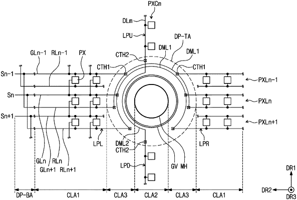
a signal line disposed on the base layer; and
an (n−1)-th pixel row and an n-th pixel row disposed on the first panel region, the (n−1)-th pixel row and the n-th pixel row are divided into at least two portions by the hole,
wherein:
the signal line comprises:
an (n−1)-th scan line electrically connected to the (n−1)-th pixel row and including a first-side line portion and a second-side line portion disposed on the first panel region, wherein the hole is disposed between the first-side line portion and the second-side line portion;
an n-th reset line electrically connected to the n-th pixel row and including a third-side line portion and a fourth-side line portion disposed on the first panel region, wherein the hole is disposed between the third-side line portion and the fourth-side line portion; and
a first row connection line disposed on the peripheral area and connecting a first-side line portion, a second-side line portion, a third-side line portion, and a fourth-side line portion;
the (n−1)-th scan line and the n-th reset line are disposed on a same layer and connected to each other via the first row connection line to receive a same signal; and
the (n−1)-th scan line and the first row connection line are disposed on different layers.
|