| CPC H10K 59/131 (2023.02) [G09G 3/3225 (2013.01); G09G 2300/0426 (2013.01); G09G 2300/0804 (2013.01); G09G 2300/0809 (2013.01); G09G 2310/0297 (2013.01); G09G 2320/04 (2013.01)] | 20 Claims |
|
1. A display panel comprising:
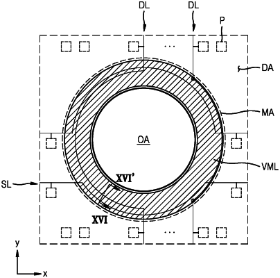
a substrate comprising a first area, a display area, and an intermediate area arranged between the first area and the display area;
a light-emitting diode in the display area and comprising a pixel electrode, an opposite electrode, and a light emitting layer between the pixel electrode and the opposite electrode;
a plurality of data lines extending along a first direction in the display area; and
a data distributor comprising switches electrically connected to the plurality of data lines,
wherein:
the plurality of data lines comprise a first data line and a second data line, a bypass portion of the first data line and a bypass portion of the second data line overlapping each other in the intermediate area; and
the bypass portion of the first data line and the bypass portion of the second data line are overlapped with a voltage layer that has a continuous ring shape completely surrounding the first area in a plan view.
|