| CPC H10K 59/131 (2023.02) [G06F 3/047 (2013.01); G06F 3/0412 (2013.01); H10K 59/121 (2023.02); H10K 59/122 (2023.02); G06F 2203/04107 (2013.01)] | 8 Claims |
|
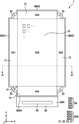
1. A display device including a display area and a non-display area, the display device comprising:
a plurality of data wires disposed in the display area and in the non-display area;
a plurality of connecting wires disposed in the display area and connected to the data wires;
a plurality of dummy patterns disposed in the display area in the same layer as the connecting wires;
a plurality of pixels disposed in the display area; and
conductive patterns disposed on the plurality of connecting wires,
wherein:
the conductive patterns include an opaque conductive material;
first gaps are defined between the plurality of connecting wires and the plurality of dummy patterns; and
the conductive patterns overlap with the first gaps;
wherein the plurality of connecting wires comprise a plurality of protruding wire patterns and the plurality of dummy patterns comprise a dummy pattern and a plurality of protruding dummy patterns;
wherein the plurality of connecting wires and the plurality of dummy patterns form a lattice pattern shape in and across the display area.
|