| CPC H10K 59/131 (2023.02) [H10K 59/121 (2023.02); H10K 59/1201 (2023.02)] | 14 Claims |
|
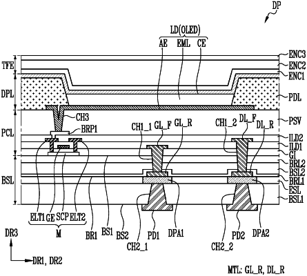
1. A display device comprising:
a base layer comprising a first surface, and a second surface;
a plurality of pixels on the first surface; and
a plurality of first lines on the first surface,
wherein the base layer comprises:
a first base layer;
an etch stop layer on the first base layer;
a plurality of second lines on the etch stop layer; and
a second base layer on the etch stop layer and the second lines,
wherein the first base layer, the etch stop layer, the second lines, and the second base layer are sequentially stacked,
wherein the first lines are electrically connected to the second lines through first contact holes, and
wherein the etch stop layer comprises conductive areas electrically connecting the second lines to a plurality of pads.
|