| CPC H10K 59/131 (2023.02) [H10K 59/122 (2023.02)] | 27 Claims |
|
1. A display substrate, comprising:
a base substrate;
an array of sub-pixels on the base substrate;
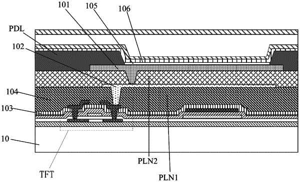
a signal line; wherein the signal line includes a first conductive pattern and a second conductive pattern which are stacked on each other, and the first conductive pattern is located between the base substrate and the second conductive pattern;
a first retaining wall structure; wherein the first retaining wall structure surrounds the array of sub-pixels; the first retaining wall structure includes a first portion and a second portion; an orthographic projection of the first portion on the base substrate does not overlap with an orthographic projection of the signal line on the base substrate; an orthographic projection of the second portion on the base substrate is partially overlapped with an orthographic projection of the first conductive pattern on the base substrate; a boundary of the orthographic projection of the second portion on the base substrate, which is distal to the array of sub-pixels, is located between an orthographic projection of the array of sub-pixels on the base substrate, and a boundary of the orthographic projection of the first conductive pattern on the base substrate, which is distal to the array of sub-pixels; the orthographic projection of the second portion on the base substrate is partially overlapped with an orthographic projection of the second conductive pattern on the base substrate; a boundary of the orthographic projection of the second conductive pattern on the base substrate, which is close to the array of sub-pixels, is located between the orthographic projection of the array of sub-pixels on the base substrate, and a boundary of the orthographic projection of the second portion on the base substrate, which is close to the array of sub-pixels.
|