| CPC H10K 59/1216 (2023.02) [H10K 59/126 (2023.02); H10K 59/1213 (2023.02); G09G 3/3233 (2013.01); G09G 2300/0426 (2013.01); G09G 2300/0465 (2013.01); G09G 2300/0842 (2013.01); H01L 27/1225 (2013.01); H01L 27/1229 (2013.01); H01L 27/1255 (2013.01)] | 12 Claims |
|
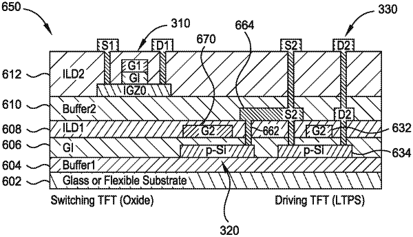
1. A sub-pixel circuit for a display, the sub-pixel circuit comprising:
a driving thin film transistor (TFT), the driving TFT comprising:
a first conductive channel in a gate insulating layer;
a first gate disposed in a first inter layer dielectric layer above the gate insulating layer;
a first source disposed in a buffer layer above the first inter layer dielectric layer and connected to the first conductive channel; and
a first drain disposed in the buffer layer and connected to the first conductive channel;
at least one switching TFT formed in a second inter layer dielectric layer above the buffer layer, wherein the at least one switching TFT is an oxide TFT; and
at least one storage capacitor, the at least one storage capacitor comprising:
a second conductive channel disposed in the gate insulating layer and isolated from the first conductive channel;
a second gate disposed in the first inter layer dielectric layer and isolated from the first gate; and
a via of the first source connected to the second conductive channel and the first source, wherein the at least one storage capacitor has a capacitance between about 1 fF and about 55 fF.
|