| CPC H10K 59/1213 (2023.02) [H10K 50/852 (2023.02); H10K 50/856 (2023.02); H10K 59/123 (2023.02); H10K 59/124 (2023.02); H10K 59/126 (2023.02); H10K 59/35 (2023.02); H10K 59/38 (2023.02); H10K 50/00 (2023.02); H10K 50/805 (2023.02); H10K 50/818 (2023.02); H10K 50/824 (2023.02); H10K 59/1201 (2023.02); H10K 59/30 (2023.02); H10K 59/351 (2023.02); H10K 2102/3026 (2023.02); H10K 2102/341 (2023.02)] | 19 Claims |
|
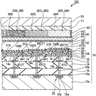
1. A light emitting device comprising:
a transistor having a gate layer;
a capacitor;
an electrode;
a first pixel electrode disposed in a layer between the transistor and the electrode;
a light emission functional layer disposed in a layer between the electrode and the first pixel electrode;
a first conductive layer disposed in a layer between the first pixel electrode and the transistor, and configured to be supplied with a constant potential;
a second conductive layer disposed in a layer between the first conductive layer and the transistor, the second conductive layer electrically connected to the transistor;
a third conductive layer disposed in a layer between the second conductive layer and the transistor, the third conductive layer electrically connected to the capacitor;
a first insulating layer disposed in a layer between the first conductive layer and the second conductive layer, the first insulating layer including a first contact hole via which the first conducive layer is electrically connected to the second conducive layer; and
a second insulating layer disposed in a layer between the third conductive layer and the transistor, the second insulating layer including a second contact hole via which the third conducive layer is electrically connected to the gate layer, wherein
in a plan view, a region where the first pixel electrode contacts with the light emission functional layer overlaps with the first conductive layer, the second conductive layer, and the third conductive layer respectively, and
in a cross-sectional view, a width of the first contact hole is wider than a width of the second contact hole.
|