| CPC H10K 50/11 (2023.02) [C07F 7/24 (2013.01); C09K 11/06 (2013.01); H10K 50/131 (2023.02); H10K 85/30 (2023.02); C09K 2211/10 (2013.01); C09K 2211/188 (2013.01); H10K 50/15 (2023.02); H10K 50/16 (2023.02); H10K 2101/40 (2023.02)] | 19 Claims |
|
1. A light-emitting device comprising:
a first electrode;
a second electrode facing the first electrode;
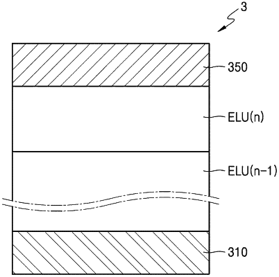
an emission layer disposed between the first electrode and the second electrode; and
a first charge transport layer disposed between the first electrode and the emission layer,
a second charge transport layer disposed between the emission layer and the second electrode,
wherein a band gap energy of the emission layer and a band gap energy of the first charge transport layer are different from each other,
wherein the band gap energy of the emission layer and a band gap energy of the second charge transport layer are different from each other,
the emission layer comprises a first perovskite compound, wherein the first perovskite compound and the second perovskite compound are different from each other; and
the first charge transport layer comprises a second perovskite compound,
wherein the band gap energy of the emission layer is less than the band gap energy of the first charge transport layer.
|