| CPC H10K 30/82 (2023.02) [H10K 85/215 (2023.02)] | 17 Claims |
|
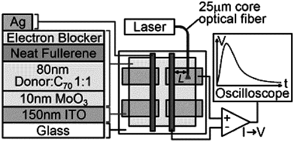
1. An optoelectronic device, comprising:
an anode;
a cathode arranged in a grid structure having a plurality of electrode segments and a respective opening between adjacent segments of the cathode;
an active layer positioned between the anode and the cathode, the active layer comprising at least one organic donor material and at least one acceptor material; and
a channel layer positioned between the cathode and the active layer, wherein the channel layer is configured to laterally disperse a charge across the channel layer;
an electron blocking layer positioned between the channel layer and the cathode, in direct contact with the channel layer and the cathode;
wherein an interface between the active layer and the channel layer has an energy barrier of at least 0.1 eV, configured to confine electrons within the channel layer.
|