| CPC H10B 99/00 (2023.02) [H01L 21/76877 (2013.01); H01L 27/088 (2013.01); H01L 29/0649 (2013.01); H01L 29/66666 (2013.01); H01L 29/7827 (2013.01)] | 12 Claims |
|
1. A method for forming a semiconductor structure, comprising:
providing a substrate, wherein a sacrificial layer and an active layer located on a surface of the sacrificial layer are formed on the substrate;
etching the active layer and the sacrificial layer up to a surface of the substrate to form a plurality of active lines arranged in parallel and extending along a first direction;
filling an opening located between two adjacent ones of the plurality of active lines to form a first isolating layer;
etching an end of each of the plurality of active lines to form opening holes exposing the surface of the substrate, a side wall of the opening holes exposing the sacrificial layer;
removing the sacrificial layer along the opening holes, to form a gap between a bottom of the plurality of active lines and the substrate;
filling a conductive material in the gap to form a bit line extending along the first direction;
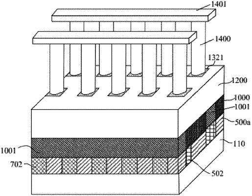
patterning the plurality of active lines to form a plurality of separate active pillars that are arrayed along the first direction and a second direction;
forming semiconductor pillars on top surfaces of respective ones of the plurality of separate active pillars;
forming a first doped region in the plurality of separate active pillars;
forming a channel region above the first doped region and a second doped region above the channel region in the semiconductor pillars; and
forming a gate structure surrounding the channel region; and
forming a second isolating layer covering the gate structure and the second doped region, the second isolating layer exposing a top surface of the second doped region.
|