| CPC H10B 63/80 (2023.02) [H10B 63/24 (2023.02)] | 20 Claims |
|
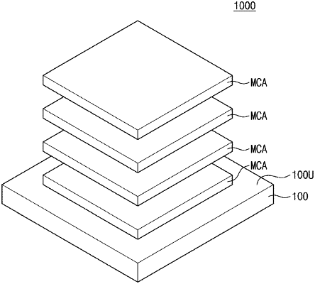
1. A variable resistance memory device, comprising:
a substrate;
memory cell structures on the substrate, the memory cell structures being spaced apart from each other in a first direction and a second direction, and the first direction and the second direction being parallel to a top surface of the substrate and intersecting each other; and
a dummy cell structure surrounding each of the memory cell structures, as viewed in a plan view, the dummy cell structure being a single body structure extending continuously between all the memory cell structures,
wherein each of the memory cell structures includes:
first conductive lines;
second conductive lines on the first conductive lines and intersecting the first conductive lines; and
memory cells between the first conductive lines and the second conductive lines, and
wherein the dummy cell structure includes:
first dummy conductive lines;
second dummy conductive lines on the first dummy conductive lines and intersecting the first dummy conductive lines; and
dummy memory cells between the first dummy conductive lines and the second dummy conductive lines.
|