| CPC H10B 43/27 (2023.02) [G11C 7/18 (2013.01); H01L 23/5226 (2013.01); H01L 24/09 (2013.01); H10B 41/10 (2023.02); H10B 41/27 (2023.02); H10B 41/35 (2023.02); H10B 41/40 (2023.02); H10B 43/10 (2023.02); H10B 43/35 (2023.02); H10B 43/40 (2023.02)] | 20 Claims |
|
1. A memory device comprising:
a lower structure; and
a plurality of upper structures stacked on the lower structure,
wherein the lower structure comprises a peripheral circuit and an upper bonding pad connected to the peripheral circuit and disposed on a top surface of the lower structure,
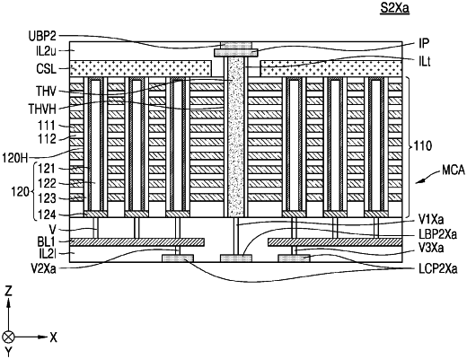
each of the plurality of upper structures has a bottom surface, and each of the plurality of upper structures comprises a stacked structure including a plurality of gate layers stacked in a vertical direction, a plurality of channel structures each passing through the stacked structure in the vertical direction, a bit line disposed under the stacked structure and connected to the plurality of channel structures, a through via passing through the stacked structure in the vertical direction, and a lower bonding pad disposed on the bottom surface and connected to the through via,
each of upper structures, other than an uppermost upper structure, of the plurality of upper structures further comprises a top surface and an upper bonding pad disposed on the top surface and connected to the through via,
the bit line of each of the plurality of upper structures comprises a first portion extending in a horizontal direction orthogonal to the vertical direction, a second portion extending in the horizontal direction, and a gap separating the first portion of the bit line from the second portion in the horizontal direction,
in a plan view, the through via of each of the plurality of upper structures overlaps the gap of the bit line,
a lowermost upper structure of the plurality of upper structures is stacked on the lower structure in the vertical direction so that the lower bonding pad of the lowermost upper structure contacts the upper bonding pad of the lower structure,
the plurality of upper structures comprise a first upper structure and a second upper structure stacked in the vertical direction, and
the lower bonding pad of the second upper structure contacts the upper bonding pad of the first upper structure,
wherein the first portion and the second portion of the bit line of at least one upper structure of the plurality of upper structures are not connected to the lower bonding pad of the at least one upper structure,
wherein the at least one upper structure comprises a first lower line connecting the lower bonding pad of the at least one upper structure to the through via of the at least one upper structure, and a second lower line connecting the first portion of the bit line of the at least one upper structure to the second portion of the bit line of the at least one upper structure and being disconnected from the lower bonding pad of the at least one upper structure, and
wherein a bottom surface of the first lower line of the at least one upper structure is disposed on a same plane as a bottom surface of the second lower line of the at least one upper structure.
|