| CPC H10B 41/50 (2023.02) [H01L 23/5226 (2013.01); H10B 41/10 (2023.02); H10B 41/27 (2023.02); H10B 43/10 (2023.02); H10B 43/27 (2023.02); H10B 43/50 (2023.02)] | 20 Claims |
|
1. A semiconductor device comprising:
a substrate including a memory cell region and a connection region; a plurality of gate electrodes stacked on the substrate;
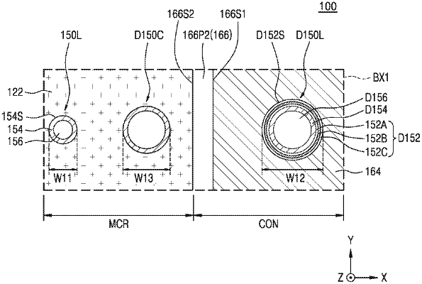
a channel structure disposed in the memory cell region and penetrating the plurality of gate electrodes, the channel structure including a channel layer extending in a vertical direction perpendicular to an upper surface of the substrate, the channel structure having a first width in a first horizontal direction;
a cell dummy channel structure disposed in the memory cell region and penetrating the plurality of gate electrodes, the cell dummy channel structure including a cell dummy channel layer extending in the vertical direction, the cell dummy channel structure having a second width greater than the first width in the first horizontal direction;
a dummy channel structure disposed in the connection region and penetrating the plurality of gate electrodes, the dummy channel structure including a dummy channel layer extending in the vertical direction, the dummy channel structure having a third width greater than the second width in the first horizontal direction;
a first semiconductor layer disposed in the memory cell region and disposed between the substrate and a lowermost gate electrode of the plurality of gate electrodes, the first semiconductor layer at least partially surrounding the channel structure and the cell dummy channel structure; and
an insulating separation structure disposed in the connection region and between the substrate and the lowermost gate electrode and at least partially surrounding the dummy channel structure.
|