| CPC H10B 41/27 (2023.02) [G11C 5/025 (2013.01); G11C 5/06 (2013.01); H01L 21/768 (2013.01); H01L 23/5384 (2013.01); H10B 43/27 (2023.02)] | 25 Claims |
|
1. A method used in forming a memory array comprising strings of memory cells, comprising:
forming a conductor tier comprising conductor material on a substrate;
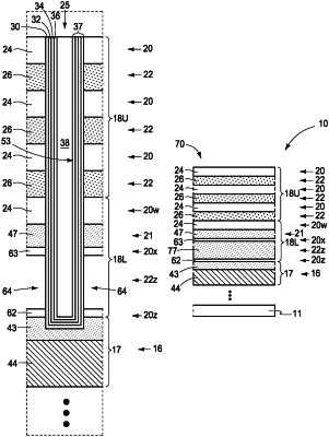
forming a lower portion of a stack that will comprise vertically-alternating first tiers and second tiers above the conductor tier, the stack comprising laterally-spaced memory-block regions, material of the first tiers being of different composition from material of the second tiers, the lower portion comprising:
a lowest of the second tiers;
a next-lowest of the second tiers directly above the lowest second tier;
a lowest of the first tiers comprising sacrificial material vertically between the lowest second tier and the next-lowest second tier; and
the lowest second tier and the next-lowest second tier comprising at least one of (a), (b), and (c), where
(a): a hafnium oxide;
(b): a bilayer comprising silicon nitride and comprising silicon dioxide positioned vertically relative one another, the silicon nitride of the bilayer being closer to the sacrificial material of the lowest first tier than is the silicon dioxide of the bilayer; and
(c): SiOxNy, where each of “x” and “y” is from 1 atomic percent to 90 atomic percent of the total of the Si, the O, and the N in the SiOxNy;
forming the vertically-alternating first tiers and second tiers of an upper portion of the stack above the lower portion, and forming channel-material strings that extend through the first tiers and the second tiers in the upper portion to the lowest first tier in the lower portion;
forming horizontally-elongated trenches through the upper portion and that extend through the next-lowest second tier to the sacrificial material of the lowest first tier, the horizontally-elongated trenches individually being between immediately-laterally-adjacent of the memory-block regions;
through the horizontally-elongated trenches, replacing the sacrificial material in the lowest first tier with conductive material that directly electrically couples together channel material of the channel-material strings and the conductor material of the conductor tier;
the lowest second tier and the next-lowest second tier comprising the (b); and
further comprising lining sidewalls of the horizontally-elongated trenches with multiple layers individually comprising one of silicon nitride or silicon dioxide and sequentially etching away the multiple layers using different etching chemistries before forming the conductive material, one of the chemistries etching the silicon nitride of the multiple layers and another of the chemistries etching the silicon dioxide of the multiple layers.
|