| CPC H10B 12/50 (2023.02) [H10B 12/315 (2023.02); H10B 12/34 (2023.02)] | 20 Claims |
|
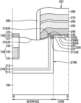
1. A semiconductor memory device comprising:
a substrate including a cell region, a core region, and a boundary region between the cell region and the core region;
a boundary element isolation layer in the boundary region, the boundary element isolation layer being in a boundary element isolation recess and including first and second boundary liner layers and a boundary element isolation filling layer; and
a first gate structure on the core region and at least a part of the boundary element isolation layer,
wherein the first boundary liner layer extends along a bottom surface of the boundary element isolation recess and sidewalls of the boundary element isolation recess,
wherein the second boundary liner layer extends on the first boundary liner layer, and comprises silicon nitride,
wherein the boundary element isolation filling layer is disposed on the second boundary liner layer,
wherein the first gate structure includes a first high dielectric layer, and a first gate insulating pattern below the first high dielectric layer, with a top surface of the substrate being a base reference level, the first gate insulating pattern does not overlap a top surface of the first boundary liner layer in a direction perpendicular to the top surface of the substrate,
wherein the first gate structure does not overlap the substrate of the cell region in the direction perpendicular to the top surface of the substrate,
wherein the first gate insulating pattern includes a first_1 gate insulating pattern between a topmost surface of the second boundary liner layer and a bottom surface of the first high dielectric layer, and a first_2 gate insulating pattern between a top surface of the substrate of the core region and a bottom surface of the first high dielectric layer, and
wherein the first_2 gate insulating pattern directly contacts the top surface of the substrate of the core region.
|