| CPC H10B 12/488 (2023.02) [H01L 21/302 (2013.01); H01L 29/66477 (2013.01); H10B 12/053 (2023.02); H10B 12/37 (2023.02); H10B 12/482 (2023.02)] | 10 Claims |
|
9. A memory, comprising:
a substrate;
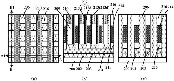
discrete bit lines located on the substrate, wherein the bit lines extend along a first direction;
discrete word lines located on the bit lines, wherein the word lines extend along a second direction, and the second direction is different from the first direction; and the word lines each has a first side wall and a second side wall opposite to each other;
an active layer, wherein the active layer is discrete and is provided between the word lines, and the active layer is located on the bit lines;
a first isolation layer, wherein the first isolation layer is provided between adjacent bit lines, between the bit lines and the word lines, and between discrete parts of the active layer;
a first dielectric layer, wherein the first dielectric layer is provided between the active layer and the first side wall; and
a second dielectric layer, wherein the second dielectric layer is provided between the active layer and the second side wall;
wherein a thickness of an equivalent-gate dielectric layer of the first dielectric layer is greater than a thickness of an equivalent-gate dielectric layer of the second dielectric layer; the first dielectric layer is of a two-layer structure, comprising an initial first dielectric layer and an initial second dielectric layer, the initial first dielectric layer covers the first side wall, and the initial second dielectric layer covers the initial first dielectric layer; a material of the initial first dielectric layer comprises a high-dielectric-constant material, and a material of the initial second dielectric layer comprises silicon oxide.
|