| CPC H10B 12/482 (2023.02) [H10B 12/0335 (2023.02)] | 21 Claims |
|
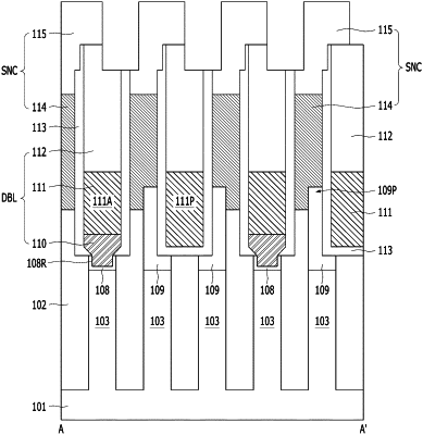
1. A semiconductor device comprising:
an active region formed in a substrate, the active region including flat surfaces and hole-shaped recess portions;
upper-level plugs disposed over the flat surfaces;
a spacer disposed between the upper-level plugs, the spacer including a trench exposing the hole-shaped recess portions;
a lower-level plug filling the hole-shaped recess portions; and
a buried conductive line disposed over the lower-level plug and partially filling the trench.
|