| CPC H10B 12/395 (2023.02) [H10B 12/0383 (2023.02); H10B 12/50 (2023.02)] | 21 Claims |
|
1. A nonvolatile memory device, comprising:
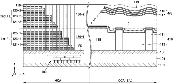
a substrate having a main chip area thereon, said main chip area including a first memory cell layer and second memory cell layer stacked on the first memory cell layer, said first memory cell layer including a first vertical channel layer, a first interlayer insulating layer, and a first gate electrode layer, and said second memory cell layer including: (i) a second vertical channel layer vertically aligned with the first vertical channel layer, (ii) a second interlayer insulating layer, and (iii) a second gate electrode layer;
an outer chip area on the substrate, which at least partially surrounds the main chip area in a portion of the substrate devoid of active devices, said outer chip layer including a step key therein that comprises an alignment vertical channel layer formed concurrently with the first vertical channel layer, said alignment vertical channel layer having a top surface that is recessed relative to the top surface of the first vertical channel layer after the first vertical channel layer is formed;
an electrically insulating layer on the second memory cell layer; and
a mold structure on the alignment vertical channel layer, said mold structure having a contoured upper surface that: (i) meets an upper surface of the electrically insulating layer, and (ii) sufficiently replicates a contoured upper surface of the outer chip area caused, at least in part, by the recessed top surface of the alignment vertical channel layer that the contoured upper surface of the mold structure can be used to support photolithographic alignment of the second vertical channel layer to the first vertical channel layer when channel layer holes are etched through the electrically insulating layer, the second interlayer insulating layer, and the second gate electrode layer;
wherein the step key further comprises an electrically insulating recessed portion, which abuts the alignment vertical channel layer; and
wherein the alignment vertical channel layer protrudes from the electrically insulating recessed portion such that the top surface of the alignment vertical channel layer is spaced farther from an underlying surface of the substrate relative to a top surface of the electrically insulating recessed portion.
|