| CPC H10B 12/36 (2023.02) [H10B 12/056 (2023.02)] | 20 Claims |
|
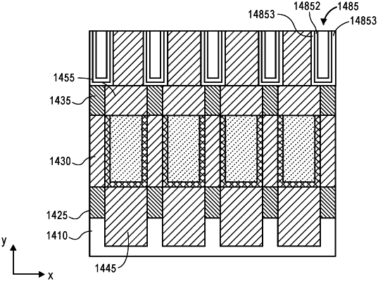
1. A method of forming an integrated circuit comprising:
forming transistor bodies in a plurality rows on a substrate, each of the bodies comprising a first diffusion region, a second diffusion region and a channel of a transistor, wherein the second diffusion regions is on the first diffusion region and separated by the channel;
forming a masking material as a plurality of rows across the bodies;
etching the bodies through the masking material to define a width dimension of the transistor bodies, wherein the width dimension is defined by a width dimension of the masking material;
after etching the bodies, patterning each of the plurality of rows of the masking material into a plurality of individual masking units comprising the width dimension and a length dimension defined by the patterning; and
replacing each of the plurality of individual masking units with a programmable element.
|