| CPC H10B 12/315 (2023.02) [H10B 12/033 (2023.02); H10B 12/05 (2023.02); H10B 12/482 (2023.02)] | 13 Claims |
|
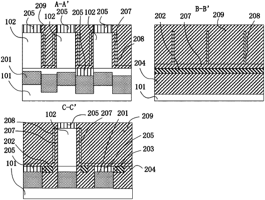
1. A memory structure, comprising:
a plurality of vertical transistors, the vertical transistors comprise silicon pillars; a plurality of the silicon pillars are arranged in m rows and n columns; the rows extend in a first direction and the columns extend in a second direction;
m bit lines, extending in the first direction and electrically connected to drains of all the vertical transistors in a same row, the drains are located below the silicon pillars; and
n word lines, extending in the second direction, located in the middle of the silicon pillars, and serving as gates of all the vertical transistors in a same column;
the first direction and the second direction form a non-right angle.
|