| CPC H10B 12/312 (2023.02) [H01L 29/6656 (2013.01); H10B 12/482 (2023.02)] | 20 Claims |
|
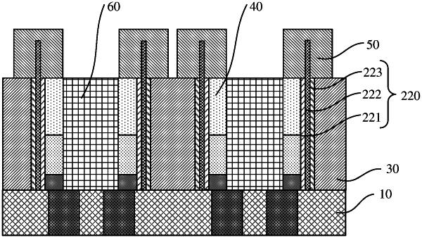
1. A manufacturing method of a semiconductor structure, comprising:
providing a substrate;
forming, on an upper surface of the substrate, first patterns each comprising a first main body and a first flank wall covering a sidewall of the first main body;
forming a filling layer which covers the first flank walls and fills a gap between adjacent first patterns; and
etching a top of each of the first patterns to obtain second main bodies, second flank walls and protrusions located on upper surfaces of the second flank walls, the second flank wall covering a sidewall of the second main body, and a top of the protrusion being at least higher than a top of the second main body.
|