| CPC H10B 12/053 (2023.02) [H10B 12/34 (2023.02)] | 6 Claims |
|
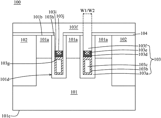
1. A method of manufacturing a memory device, comprising:
providing a semiconductor substrate defined with an active area and including an isolation structure surrounding the active area;
forming a recess extending into the semiconductor substrate and across the active area;
forming a first insulating layer conformal to the recess;
disposing a first conductive material conformal to the first insulating layer;
forming a conductive member surrounded by the first conductive material;
disposing a second conductive material over the conductive member and removing a portion of the first conductive material above the second conductive material to form a conductive layer enclosing the conductive member; and
forming a second insulating layer over the conductive layer and conformal to the first insulating layer;
wherein a top surface of the second insulating layer is substantially lower than a top surface of the first insulating layer and a top surface of the semiconductor substrate.
|