| CPC H10B 10/12 (2023.02) [G11C 11/412 (2013.01); G11C 11/417 (2013.01)] | 6 Claims |
|
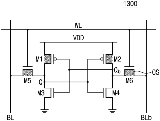
1. A static random-access memory (SRAM) device comprising:
a substrate including a PMOS area;
a circuit wiring structure including an insulating layer and a wiring layer alternately stacked on the substrate, wherein the circuit wiring structure comprises a first NMOS area and a second NMOS area vertically separated from the PMOS area with the first NMOS area therebetween;
a first transistor including a first gate electrode disposed on the PMOS area, source/drain areas formed on the PMOS area on both sides of the first gate electrode, and a first channel connecting the source and drain areas to each other;
a second transistor including a second gate electrode disposed in the first NMOS area and a second channel vertically overlapping the second gate electrode; and
a third transistor including a third gate electrode disposed in the second NMOS area and a third channel vertically overlapping the third gate electrode,
wherein the first channel comprises silicon,
wherein the second channel and the third channel comprise an oxide semiconductor.
|