| CPC H05K 7/20963 (2013.01) [G09F 9/301 (2013.01); G06F 3/0412 (2013.01); G06F 3/04164 (2019.05); G06F 2203/04102 (2013.01)] | 14 Claims |
|
1. A curved electronic device, comprising:
a substrate;
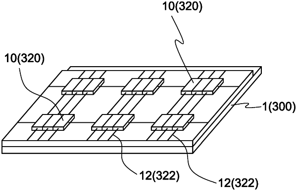
a component layer, disposed on the substrate, the component layer being composed of a plurality of electronic components and their connecting wiring arranged on the substrate; and
a modulation layer, disposed on the component layer and including at least one pattern area and at least one blank area that are formed on the component layer, wherein the blank area allows one part of the electronic components to be exposed out of the modulation layer, a position of the substrate corresponding to the pattern area and a position of the substrate corresponding to the blank area have different heat absorption rates.
|