| CPC H05K 1/144 (2013.01) [H05K 1/115 (2013.01); H05K 1/181 (2013.01); H05K 3/341 (2013.01); H05K 3/36 (2013.01); H01L 23/473 (2013.01)] | 47 Claims |

|
1. A hybrid double-sided power switch module, comprising:
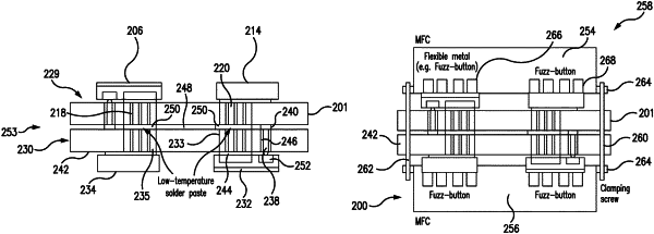
a first printed circuit board (PCB) and a second PCB, wherein said first PCB has a first side and a second side opposite to said first side, and wherein said second PCB has a third side and a fourth side opposite to said third side of said second PCB, said first and second PCBs being configured with at least first and second through-hole-vias (THVs), said first THV extending between said first and second sides of said first PCB, and said second THV extending between said third and fourth sides of said second PCB;
at least one first switch die secured to said first side of said first PCB with a gate terminal of said at least one first switch die facing said first side of said first PCB in alignment with said first THV formed through said first PBC, and
at least one first spring pin soldered inside said first THV formed through said first PCB by a high-temperature solder paste, said at least one first spring pin having a first conductive body with a first cap formed at one end of said first conductive body and a second cap formed at another end of said first conductive body, wherein said at least one first spring pin has said first cap aligned and in contact with said gate terminal of said at least one first switch die, and wherein said second cap is exposed at said second side of said first PCB in alignment and contact with said first THV formed through said first PCB; and
at least one second switch die secured to said third side of said second PCB with a gate terminal of said at least one second switch die facing said third side of said second PCB in alignment with said second THV formed through said second PCB, and
at least one second spring pin soldered inside said second THV formed through said second PCB by said high-temperature solder paste, said at least second spring pin having a second conductive body with a third cap formed at one end of said second conductive body and a fourth cap formed at another end of said second conductive body, wherein said at least one second spring pin has said third cap aligned and in contact with said gate terminal of said at least one second switch die, and wherein said fourth cap is exposed at said fourth side of said second PCB in alignment and in contact with said second THV formed through said second PCB;
wherein said first and second PCB s are secured to one another by a low-temperature solder paste with said second and fourth sides thereof facing each other, thus forming a double PCB assembly with said at least one first switch die and said at least one second switch die secured at said first and third sides interconnected to configure the power switch module of a predetermined configuration.
|