| CPC H05K 1/118 (2013.01) [G01R 27/08 (2013.01); H01L 27/124 (2013.01); H05K 1/0268 (2013.01); H05K 2201/10128 (2013.01)] | 22 Claims |
|
1. An electronic apparatus comprising:
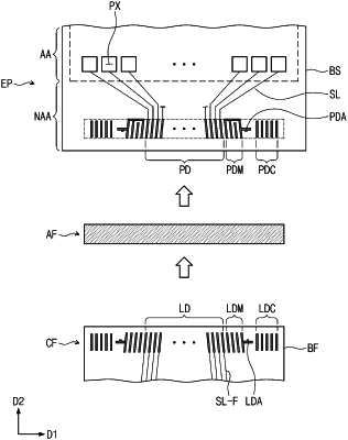
an electronic panel comprising a base substrate, a plurality of pixels on the base substrate, and a plurality of pads in an adhesive area, the plurality of pads is spaced apart from the plurality of pixels;
a circuit board comprising a base film, and a plurality of leads disposed on the base film and overlapping the plurality of pads in a plan view; and
a conductive adhesive member disposed on the adhesive area and configured to electrically connect the circuit board and the electronic panel,
wherein the plurality of pads comprises a plurality of pixel pads electrically connected to the plurality of pixels, an arrangement pad spaced apart from the plurality of pixel pads, and a resistance measurement pad disposed between the arrangement pad and the plurality of pixels pads and insulated from the plurality of pixel pads, and
the plurality of leads comprises a plurality of pixel leads overlapping the plurality of pixel pads in the plan view, an arrangement lead overlapping the arrangement pad in the plan view, and a resistance measurement lead disposed between the plurality of pixel leads and the arrangement lead and insulated from the plurality of pixel leads,
wherein the resistance measurement lead comprises a plurality of resistance measurement leads disposed between the arrangement lead and the plurality of pixel leads and electrically connected to the resistance measurement pad, and a dummy lead spaced apart from each of the plurality of resistance measurement leads in the plan view.
|