| CPC H05K 1/116 (2013.01) [H05K 1/0222 (2013.01); H05K 2201/0195 (2013.01); H05K 2201/09509 (2013.01)] | 11 Claims |
|
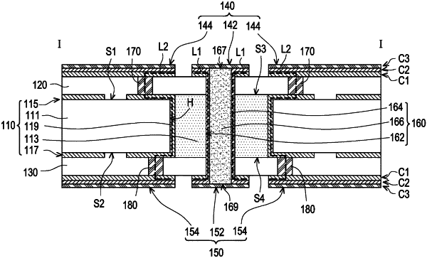
1. A circuit board structure, comprising:
a substrate having an opening and comprising a first dielectric layer, a second dielectric layer, a first inner circuit layer, a second inner circuit layer, and a conductive connection layer, wherein the opening penetrates through the first dielectric layer, the first dielectric layer has a first surface and a second surface opposite to each other, the first inner circuit layer is disposed on the first surface, and the second inner circuit layer is disposed on the second surface, the conductive connection layer covers an inner wall of the opening and connects the first inner circuit layer and the second inner circuit layer, the second dielectric layer fills the opening, and the second dielectric layer has a third surface and a fourth surface opposite to each other;
a third dielectric layer covering the first inner circuit layer and the third surface;
a fourth dielectric layer covering the second inner circuit layer and the fourth surface;
a first external circuit layer disposed on the third dielectric layer;
a second external circuit layer disposed on the fourth dielectric layer;
a conductive through hole penetrating through the third dielectric layer, the second dielectric layer, and the fourth dielectric layer, and connecting the first external circuit layer and the second external circuit layer electrically;
a first annular retaining wall disposed in the third dielectric layer, surrounding the conductive through hole, and connecting the first external circuit layer and the first inner circuit layer electrically; and
a second annular retaining wall disposed in the fourth dielectric layer, surrounds the conductive through hole, and connecting the second external circuit layer and the second inner circuit layer electrically.
|