| CPC H05K 1/113 (2013.01) [H05K 2201/096 (2013.01)] | 20 Claims |
|
1. A printed circuit board comprising:
a first insulating layer;
a second insulating layer disposed on the first insulating layer;
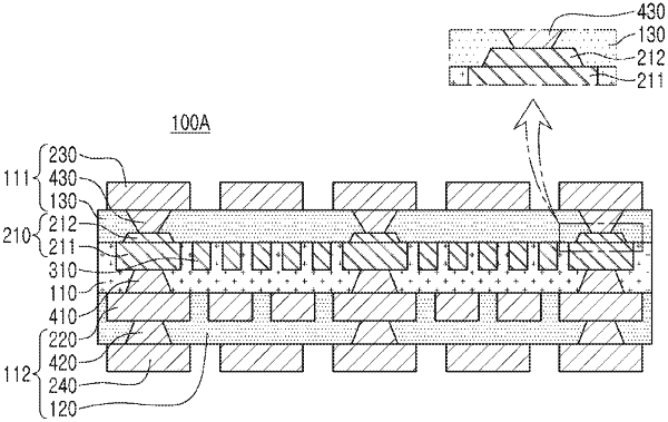
a via pad including a first layer embedded in the first insulating layer and a second layer disposed on the first layer and embedded in the second insulating layer, the second layer directly contacting the first layer; and
a first via layer disposed on one side of the via pad, connected to the first layer and penetrating through at least a portion of the first insulating layer, and a second via layer disposed on an opposing side of the via pad, connected to the second layer and penetrating through at least a portion of the second insulating layer,
wherein the second layer has a width decreasing in a direction away from the first layer in a stacking direction of the first and second layers,
each of the first and second layers of the via pad includes a metal material,
the second via layer is in contact with the second layer and has a tapered side surface, and
each of the first and second insulating layers is a single layer.
|