| CPC H04N 25/709 (2023.01) [H04N 25/75 (2023.01); H01L 27/1463 (2013.01); H01L 27/14609 (2013.01)] | 21 Claims |
|
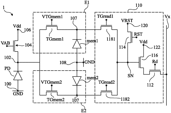
1. An image sensor comprising:
an array of pixels arranged inside and on top of a region of a semiconductor substrate electrically insulated from a remainder of the substrate by insulating trenches crossing the substrate, wherein each pixel comprises a photoconversion area and at least two assemblies, wherein each assembly comprises a memory area and a transfer gate coupling the memory area to the photoconversion area; and
a first circuit configured to apply, for each pixel and at least during each integration phase, a first bias voltage different from a ground potential to a portion of the substrate having the pixel arranged inside and on top of it, wherein the first bias voltage is a positive voltage.
|