| CPC H04N 25/46 (2023.01) [H01L 27/14607 (2013.01); H04N 25/76 (2023.01)] | 15 Claims |
|
1. A solid-state imaging device, comprising:
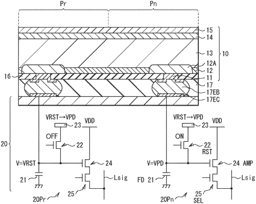
a photoelectric conversion film provided over a plurality of pixels, wherein the plurality of pixels include readout pixels and non-readout pixels with a fixed arrangement;
a first electrode electrically coupled to the photoelectric conversion film and provided to each pixel;
a passivation film disposed between an interlayer insulating layer and a semiconductor layer, wherein the first electrode is provided in the passivation film and a portion of the first electrode is provided in the interlayer insulating layer;
a second electrode opposed to the first electrode, the photoelectric conversion film being interposed between the second electrode and the first electrode;
a first electric charge accumulation section that accumulates signal electric charges which are generated in the photoelectric conversion film and are moved via the first electrode;
a reset transistor that is provided to each pixel and applies a reset electric potential to the first electric charge accumulation section;
a transistor for switching a capacitance; and
an additional capacitance element that is coupled to the transistor.
|