| CPC H04N 25/42 (2023.01) [G01S 7/4914 (2013.01); H04N 25/772 (2023.01); G01S 17/08 (2013.01)] | 6 Claims |
|
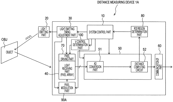
1. An imaging device, comprising:
a plurality of pixels configured to receive reflected light from a target region, wherein
the plurality of pixels is in a matrix arrangement,
each pixel of the plurality of pixels includes:
a light receiving element configured to output an electric signal based on a charge, and
a first accumulation part and a second accumulation part,
the charge is accumulated in one of the first accumulation part or the second charge accumulation part based on the reflected light;
a control part configured to execute switching control of the first accumulation part and second charge accumulation part by switching frequencies for each pixel region, wherein
the switching frequencies are different from each other,
the execution of the switching control of the first accumulation part and the second charge accumulation part is based on a determination result of a region of interest of the imaging frame,
the switching control of the first accumulation part and second charge accumulation part is between the region of interest and a region different from the region of interest,
the determination result of the region of interest of the imaging frame is supplied from an external device,
each pixel region is constituted of a pixel group,
the pixel group is of at least one part of an imaging frame, and
the pixel group comprises the plurality of pixels.
|