| CPC H04N 25/40 (2023.01) [H04N 25/77 (2023.01)] | 11 Claims |
|
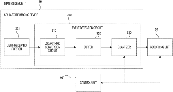
1. An imaging device, comprising:
a solid-state imaging device including:
a plurality of pixels each including a light-receiving portion that photoelectrically converts incident light to generate an electrical signal, and
a detection circuit configured to:
execute event signal detection by comparing an amount of change in the electrical signal generated by the light-receiving portion with a specific threshold value to obtain a detection result; and
execute, as the event signal detection, on event signal detection by comparing the amount of change in the electrical signal generated by the light-receiving portion with a first threshold value to obtain the detection result, and off event signal detection by comparing the amount of change in the electrical signal generated by the light-receiving portion with a second threshold value to obtain the detection result; and
a control unit configured to execute control so that different pixel groups have different timing for an event detection period to cause the detection circuit to execute the event signal detection, wherein
the control is executed on the detection circuit of each pixel in a detection cycle including an on event detection period to cause the on event signal detection to be executed, an off event detection period to cause the off event signal detection to be executed, a reset period, and an event read period, and
the control is executed so that when the detection circuit in each pixel of a first pixel group is in the on event detection period, the detection circuit in each pixel of a second pixel group is in the off event detection period.
|