| CPC H04N 23/667 (2023.01) [B60R 1/22 (2022.01); H04N 23/61 (2023.01)] | 14 Claims |
|
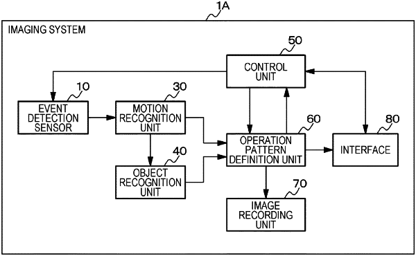
1. An imaging device comprising:
an event detection sensor configured to detect an event, wherein the event detection sensor includes an asynchronous imaging device that detects as an event that a change in brightness in a pixel that photoelectrically converts incident light exceeds a predetermined threshold value; and
a processor configured to:
control the event detection sensor, and switch a resolution of the event detection sensor depending on a traveling state of a mobile body, wherein the imaging device is mounted on the mobile body; and
set the resolution of the event detection sensor to a first resolution mode in which the resolution is relatively low or a second resolution mode in which the resolution is relatively high, depending on the traveling state of the mobile body.
|